


If you Entered The Select Menu

본문
Then again, for low-frequency applications, the conflicting requirement of avoiding ground loops mandates that the shield should only be linked at one side. Thus, the shield is often related at one finish, and disconnected at the opposite facet. Chassis ground and signal ground are often related collectively at a number of points. I/O cover. When the board is installed, the I/O cowl is pushed forcefully onto the chassis. When the cage is zapped by ESD, though absolutely the potential of the circuit relative to the Earth ground will increase, the relative potentials stay the same, and the circuit board is perfectly protected. This sacrifices efficient RF shielding, lowering the Faraday cage that is able to blocking high-frequency radiation to a easy electrostatic display, only capable of blocking low-frequency electric fields, like mains hum. This all sounds fairly nice - maybe you’d like to document it? To mitigate this drawback, Ott recommends creating a separate space on the circuit board, devoted to I/O connectors. Mount the connector onto the chassis, making a stable shield-to-chassis termination. In an old-college design the connectors are screwed onto the chassis, so a shield-to-chassis connection is almost all the time the prefered path for noise current.
The shield-to-chassis connection must be the preferred path of the RF noise present. Connecting the shield at each ends create a floor loop, a small difference of ground potential causes a noise present to stream from one end to a different. Coincidentally, this downside also occurs at a a lot better scale in industrial installations across buildings the place a big difference of "Earth" potential between locations exist. Any small noise voltage attributable to a distinction in floor potential that may couple into the circuit (primarily at energy line frequencies and its harmonics) is not going to affect digital circuits and may normally be filtered out of rf circuits, because of the big frequency distinction. In the case of a coaxial cable, the shield present will produce a noise voltage whose magnitude is equal to the shield current instances the shield resistance, as was proven in Eq. The decrease the worth of the board ground to chassis impedance, the smaller the widespread-mode present on the cable will probably be.
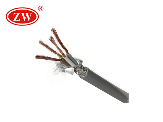
At this I/O space, a solid connection is made between the chassis and the circuit floor, concurrently, the cable shield is terminated to the chassis at the same location. One full flip clockwise will advance the tension vary approximately 1.0 - 2.5 lbs, a counter-clockwise flip will decrease tension by the identical amount. If the circuit ground is connected to the chassis at the end of the PCB opposite the cable, then the full voltage VG will drive the present onto the cable. The precise implementation of an effective hybrid cable shield ground could, however, be difficult, as a result of any inductance in collection with the capacitor will lower its effectiveness. However, at excessive frequency, the capacitor becomes a low impedance, which converts the circuit to 1 that is grounded at both ends. At low frequency, shield control cable a single-point floor exists because the impedance of the capacitor is massive. Use numerous SMD capacitors to connect the chassis and shield. This essentially mandates the termination of shield and chassis at each sides. The inside shield can then be terminated at just one end, thus avoiding the bottom-loop coupling that may happen if grounded at each ends. If one aspect just isn't appropriately designed, sometimes past our control, a common-mode noise present flows and creates increased interference, as beforehand described.
If terminating the shield at both sides is required for prime-frequency shielding, while terminating the shield at one facet is required for low-frequency analog techniques to avoid mains hum. This presumably explains the reason that disconnecting the USB shield at one facet just isn't a deal-breaker, despite that it isn't elegant in theory. In my authentic answer, I believed I already carefully navigated around the nuisances of the pros and cons of connecting the shield at one aspect, or at both sides. Using analog and combined-signal circuits in USB machine, similar to audio or knowledge acquisition, could rule out connecting the shield at each sides as an possibility, compromising RF shielding. Combined with some combined-signal or analog circuits on the board which might be vulnerable to floor loop, the scenario becomes a total mess. Because of the movement of present, there exists a voltage gradient across the circuit floor airplane of the circuit board. 1. The receptacle shell shall be linked to the PCB floor plane.
댓글목록0
댓글 포인트 안내